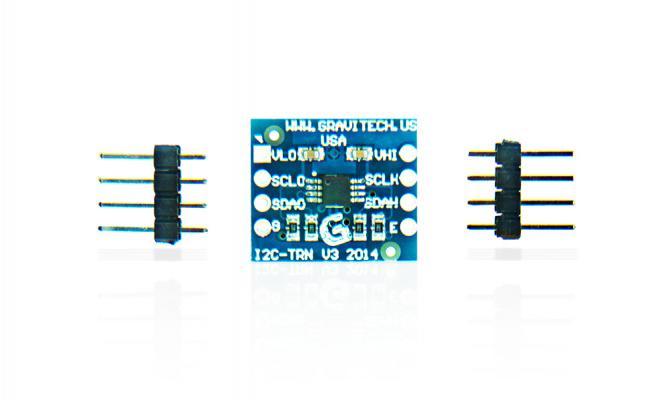
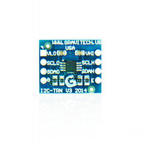
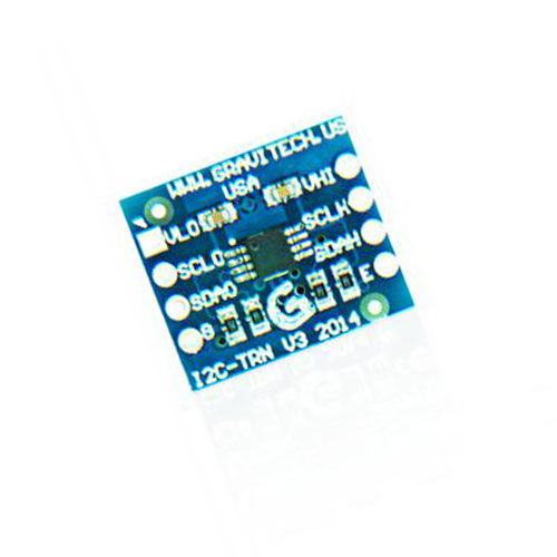


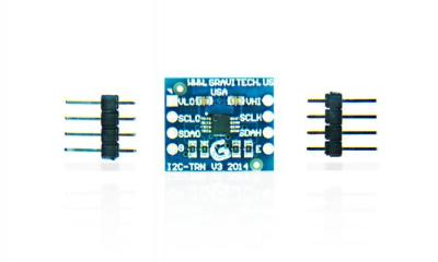
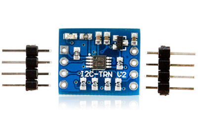
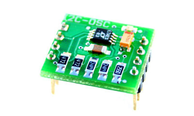
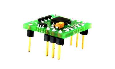
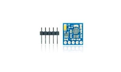
Bidirectional I2C Voltage-Level Translator v3.0 (PCA9617A)
เป็นอุปกรณ์แปลงระดับแรงดันที่มีความรวดเร็วและมีความแม่นยำสูงใน version 3.0 นี้เราได้ใช้ IC PCA9617A กับการจัดรูปแบบวงจรที่ลงตัวจะทำให้การติดต่อ I2C ของคุณมีความถูกต้องมากยิ่งขึ้น ด้วยการเพิ่ม bufferให้ทั้งสาย SDA และ SCL คุณจะได้ค่า HIGH และ LOW ที่ถูกต้องรองรับความเร็ว clock 0 Hz ถึง 1000 kHz แปลงระดับลอจิกได้ตั้งแต่ 0.8V ถึง 5.5V ในช่วงแรงดันต่ำ และ 2.2V ถึง 5.5V ในช่วงแรงดันที่สูงกว่า เหมาะสำหรับการติดต่อสื่อสารกันเซ็นเซอร์ต่างๆที่ใช้ระดับแรงดันของลอจิกที่แตกต่างกัน
General description
The PCA9617A is a CMOS integrated circuit that provides level shifting between low voltage (0.8 V to 5.5 V) and higher voltage (2.2 V to 5.5 V) Fast-mode Plus (Fm+) I2C-bus or SMBus applications. While retaining all the operating modes and features of the
I2C-bus system during the level shifts, it also permits extension of the I2C-bus by providing bidirectional buffering for both the data (SDA) and the clock (SCL) lines, thus enabling two buses of 540 pF at 1 MHz or up to 4000 pF at lower speeds. Using the PCA9617A enables the system designer to isolate two halves of a bus for both voltage and capacitance. The SDA and SCL pins are overvoltage tolerant and are high-impedance when the PCA9617A is unpowered.
The 2.2 V to 5.5 V bus port B drivers have the static level offset, while the adjustable voltage bus port A drivers eliminate the static offset voltage. This results in a LOW on the port B translating into a nearly 0 V LOW on the port A which accommodates the smaller voltage swings of lower voltage logic.
The static offset design of the port B PCA9617A I/O drivers prevents them from being connected to the static or incremented offset of other bus buffers. Port A of two or more PCA9617As can be connected together, however, to allow a star topography with port A on the common bus, and port A can be connected directly to any other buffer with static or incremented offset outputs. Multiple PCA9617As can be connected in series, port A to
port B, with no build-up in offset voltage with only time of flight delays to consider. The PCA9617A drivers are not enabled unless VCC(A) is above 0.8 V and VCC(B) is above 2.2 V. The EN pin is referenced to VCC(B) and can also be used to turn the drivers on and off under system control. Caution should be observed to only change the state of the enable pin when the bus is idle.
The output pull-down on the port B internal buffer LOW is set for approximately 0.55 V, while the input threshold of the internal buffer is set about 90 mV lower (0.45 V). When the port B I/O is driven LOW internally, the LOW is not recognized as a LOW by the input. This prevents a latching condition from occurring. The output pull-down on port A drives a hard LOW and the input level is set at 0.35VCC(A) to accommodate the need for a lower LOW level in systems where the low voltage side supply voltage is as low as 0.8 V.
Features and benefits
♦ 2 channel, bidirectional buffer isolates capacitance and allows 540 pF on either side of the device at 1 MHz and up to 4000 pF at lower speeds
♦ Voltage level translation from 0.8 V to 5.5 V and from 2.2 V to 5.5 V
♦ Footprint and functional replacement for PCA9517A at Fast-mode speeds
♦ Port A operating supply voltage range of 0.8 V to 5.5 V with normal levels
♦ Port B operating supply voltage range of 2.2 V to 5.5 V with static offset level
♦ 5 V tolerant I2C-bus and enable pins
♦ 0 Hz to 1000 kHz clock frequency (the maximum system operating frequency may be less than 1000 kHz because of the delays added by the repeater)
♦ Active HIGH repeater enable input referenced to VCC(B)
♦ Open-drain input/outputs
♦ Latching free operation
♦ Supports arbitration and clock stretching across the repeater
♦ Accommodates Standard-mode, Fast-mode and Fast-mode Plus I2C-bus devices, SMBus (standard and high power mode), PMBus and multiple masters
♦ Powered-off high-impedance I2C-bus pins
♦ ESD protection exceeds 5500 V HBM per JESD22-A114 and 1000 V CDM per JESD22-C101
♦ Latch-up testing is done to JEDEC Standard JESD78 which exceeds 100 mA
♦ Packages offered: TSSOP8 and HWSON8
• มีบัฟเฟอร์ทำให้สามารถใช้งานได้ 2 ทิศทาง
• แปลงระดับแรงดันจาก 0.8 V เป็น 5.5 V และจาก 2.2 V เป็น 5.5 V
• ใช้ IC PCA9617A ที่มีความเร็วในการทำงานสูง
• ทำจาก PCB คุณภาพสูง (soldermask สีฟ้า)
• ความถี่สัญญาณนาฬิกา 0 เฮิร์ทซ์ ถึง 1000 เฮิร์ทซ์
• ป้องกัน ESD (Electrostatic Discharge) 5500 V HBM ต่อ JESD22-A114 และ 1000 CDM V ต่อ JESD22-C101
• บอร์ดขนาด 0.70 x 0.57 นิ้ว
•ใช้งานร่วมกับโปรโตบอร์ดได้
• PCB ที่มีคุณภาพสูง (soldermask สีฟ้า)
• 5 V tolerant I2C-bus และ enable pins
• Active HIGH repeater enable input อ้างอิงที่ VCC(B)
• Open-drain input/outputs
• Latching free operation
• Supports arbitration and clock stretching across the repeater
• รองรับอุปกรณ์ที่ Standard-mode Fast-mode และ Fast-mode Plus I2C-bus, SMBus (standard and high power mode), PMBus และ multiple masters
• Powered-off high-impedance I2C-bus pins
• Latch-up ทดสอบแล้วที่ JEDEC Standard JESD78 ที่เกินกว่า 100 mA
• Packages offered: TSSOP8 and HWSON8


![ใหม่ [0493] ไม้ปัดฝุ่นไมโครไฟเบอร์ แบบยืดสไลด์ได้ สําหรับรถยนต์](https://down-th.img.susercontent.com/file/id-11134201-7qul1-ljlinh0xspxff0_tn)